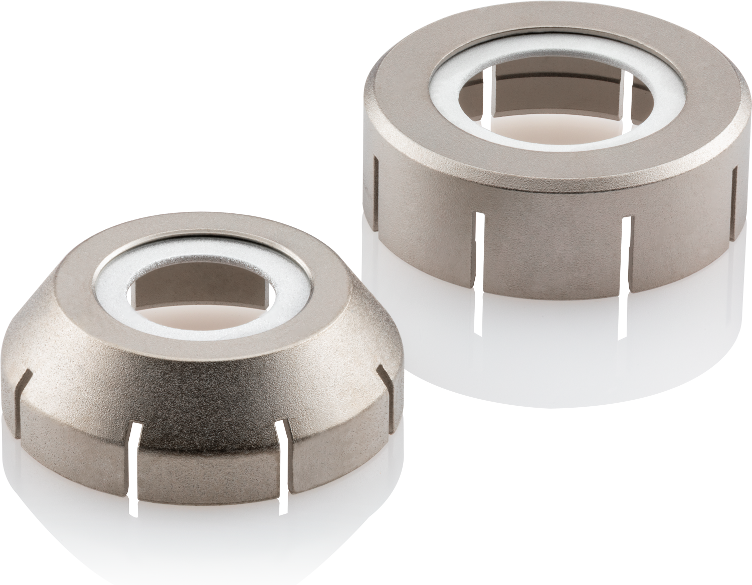
AXAS 3.0
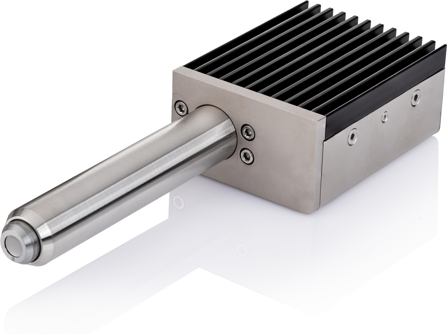
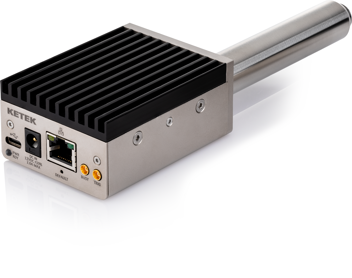
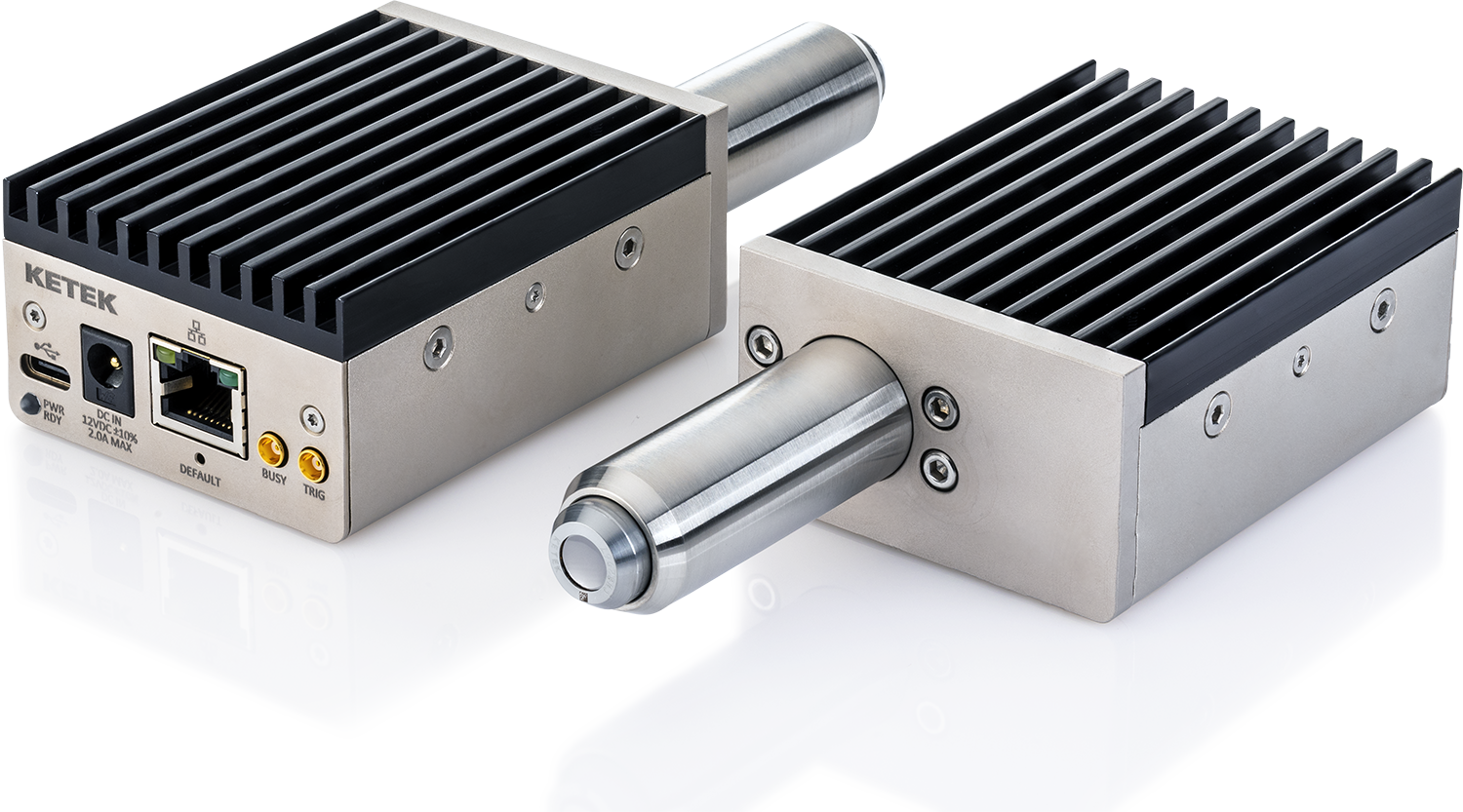
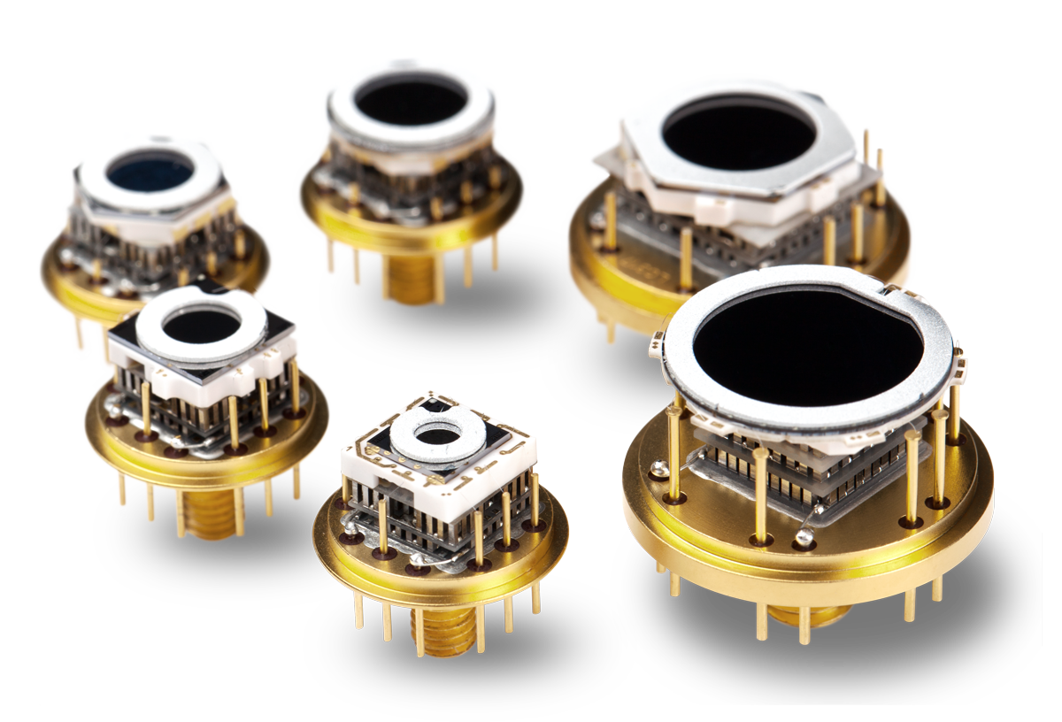
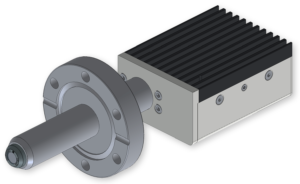
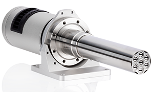
The new AXAS 3.0 is a complete spectroscopic system for VITUS SDDs in a very compact housing. It includes all power supplies, the latest generation preamplifier, a high precision temperature controller and in the digital system KETEK‘s proprietary digital pulse processor DPP3. The AXAS 3.0 is available with all sizes of VITUS SDDs from H7 to H50 and different lengths of the vacuum tight finger.
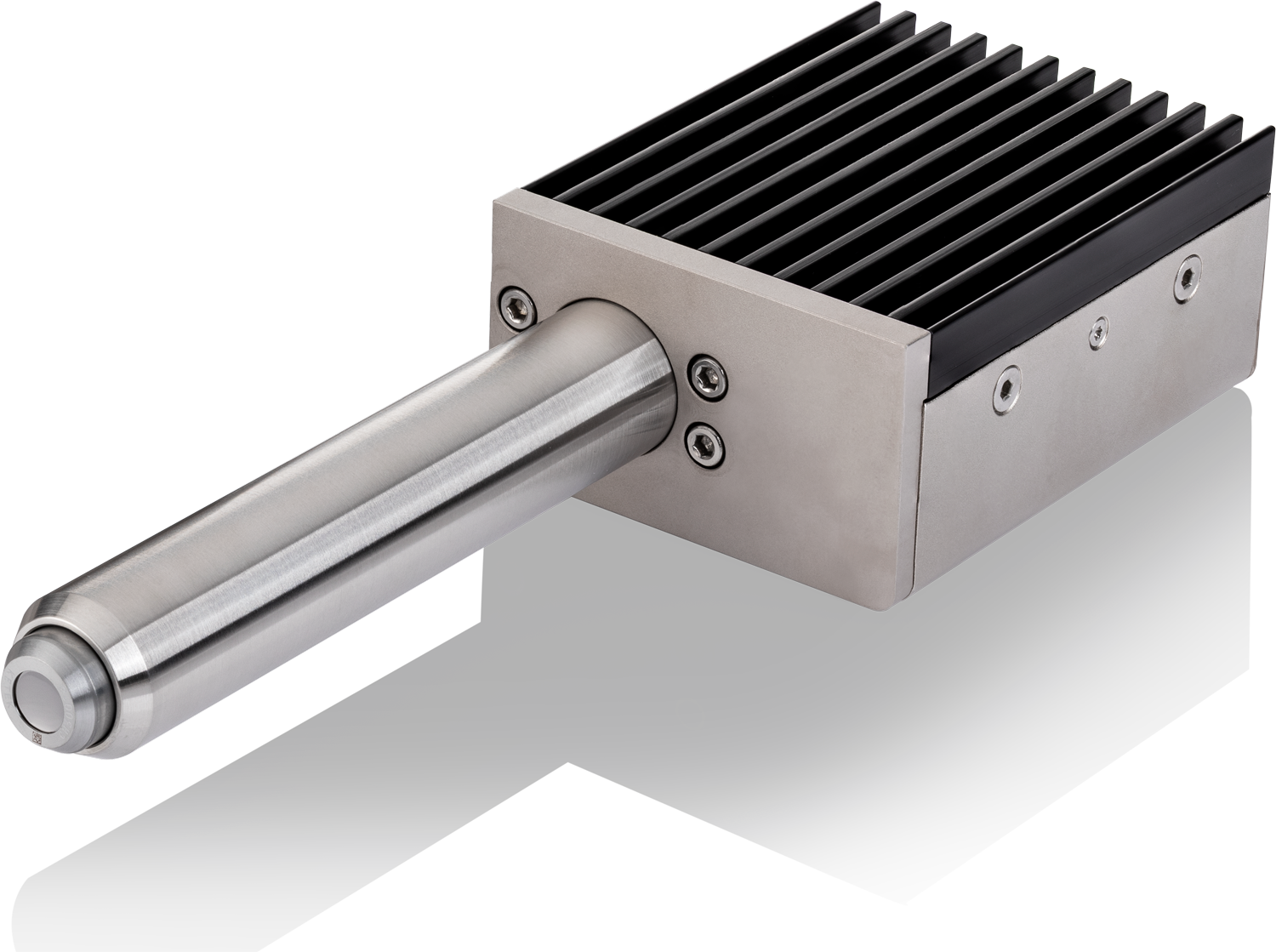
AXAS 3.0
Complete system for VITUS modules H7 to H50
Unique Features
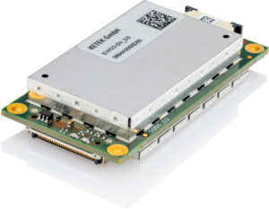
- KETEK‘s new high-performance digital pulse processor DPP3 with peaking time down to 25 ns
- Latest Generation 3.0 Preamp technology
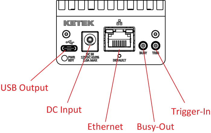
- Ethernet and USB 2.0 Type-C interface
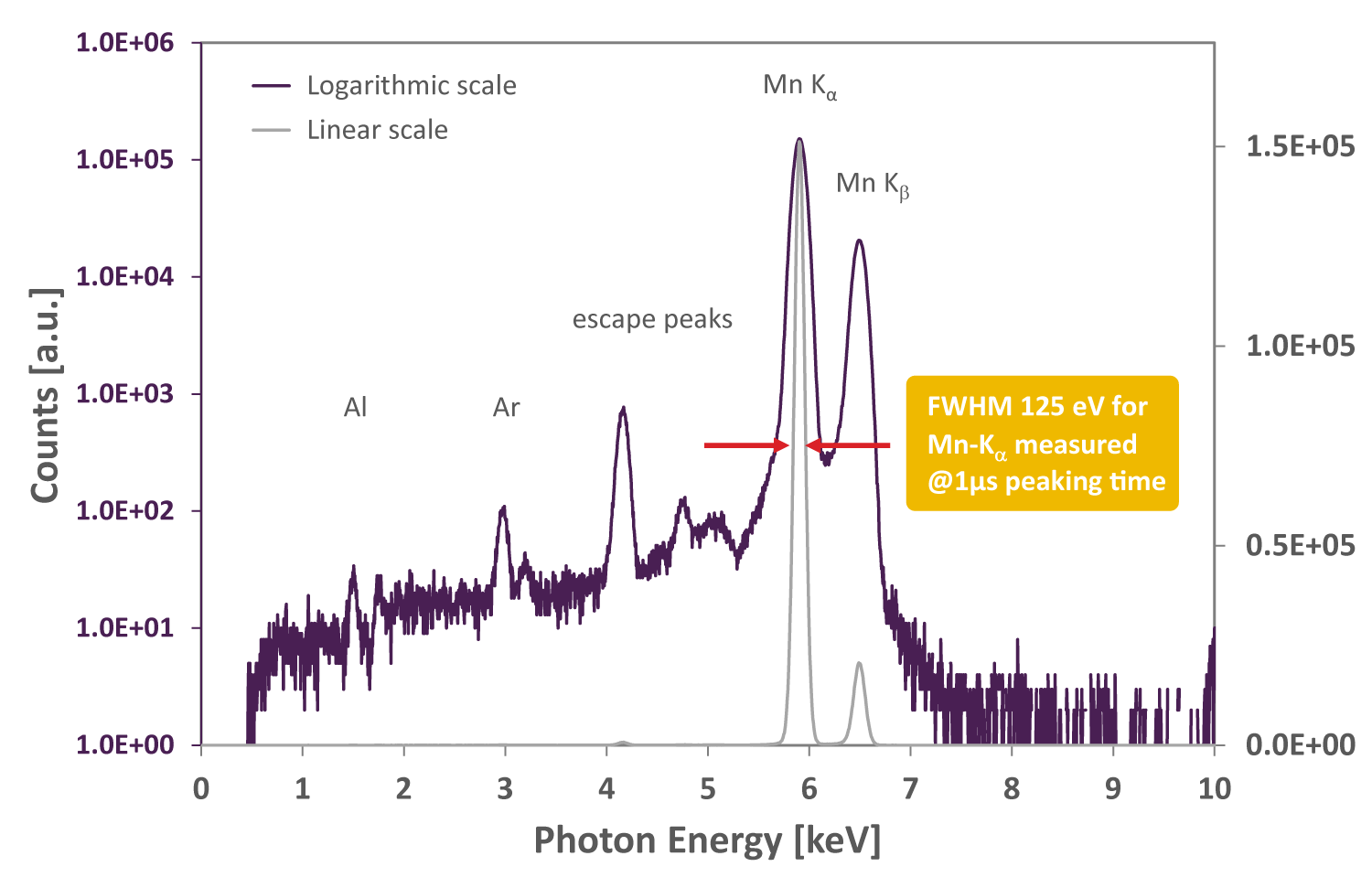
- Guaranteed: FWHM < 133 eV @ 1 µs peaking time for Mn Kα line
- Both Graphene window types available
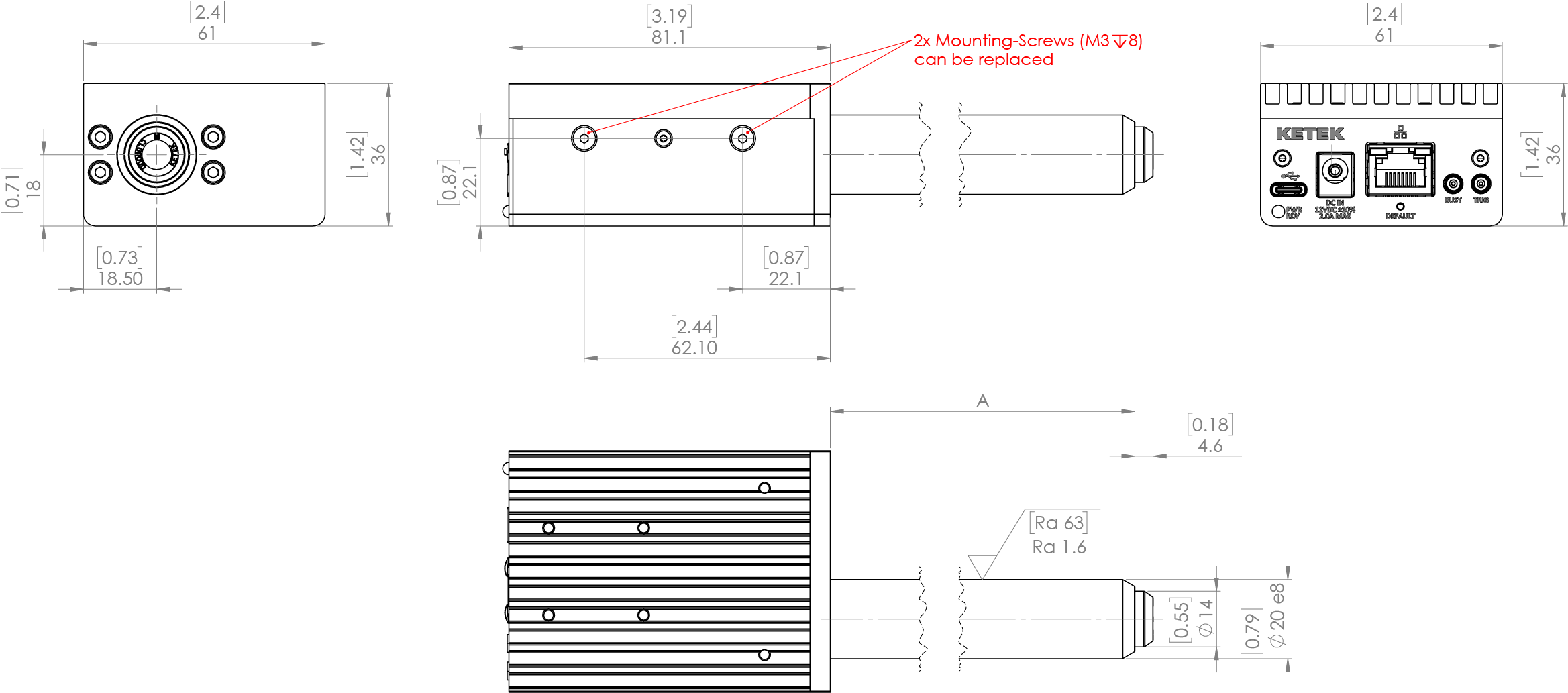
- Extremely small form factor: 81 × 61 × 36 mm³ (AXAS body only)
- Single supply voltage: + 12 VDC / 250 mA typ
- Support for EPICS control system
- DLLs for Windows and libraries for LINUX, ARM based machines supported
- Four M3 screws for easy mounting in customer system
- Finger configuration compatible with previous AXAS 2.0
Available Options
Specifications
| First amplification stage | KETEK CSA |
| Energy resolution (@ Mn Kα, -35 °C chip temperature and 1 µs peaking time) | ≤ 133 eV |
| Peak to background | > 15,000 |
| Peak to tail | > 2,000 |
| Peak shift stability up to 100 kcps | < 1 eV |
| Max. input countrate | 4,000 kcps |
| Graphene CH window
Graphene CL window |
1 µm Carbon
165 nm Carbon |
| Cooling performance at +20 °C heat sink temperature |
∆T > 85 K |
Spectrum
Energy Resolution
This plot shows the energy resolution for Mn Kα measured with a AXAS-D 3.0 with a VITUS H50 CH at two different SDD chip temperatures. The included KETEK DPP3 allows peaking times down to 25 ns. The best set of parameters depend on the application optimizing either the energy resolution or the achievable through put.
Throughput
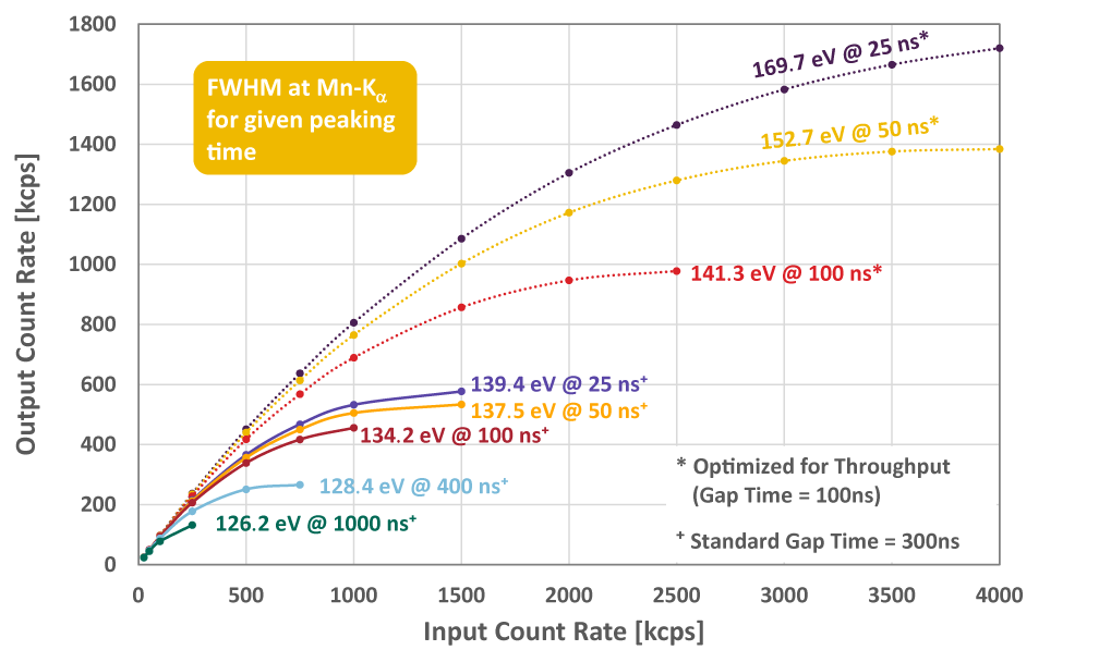
The graph shows the throughput curves of the KETEK DPP3 and the concerning energy resolution for Mn Kα measured with a VITUS H20 SDD at different peaking times between 25 ns and 2 µs. The standard parameters are optimized for high energy resolution (gap time = 300 ns). The parameters for optimized throughput use a shorter gap time (gap time = 100 ns).
Technical Data
| Parameter | Specification | Note |
| Dimensions | 81 x 61 x 36 mm³ | |
| Finger Length [A] | 50 mm, 100 mm or 200 mm | Other finger lengths available on request. System dimensions with finger length A under section Geometry. |
| Weight | 0.58 kg ± 0.01 kg | with 100 mm finger length |
| Operating Temperature Range | 0 °C to +50 °C | |
| Storage Temperature Range | -20 °C to +50 °C | |
| Operating Humidity Range | 10 to 80 % | non-condensing |
| SDD temperature monitor | Digital temperature read-out | |
| Vacuum tightness | He leakage rate < 10-9 mbar · l/s | |
| DC Input Voltage | +12 V ± 10 % | |
| DC Input Current | +600 mA max. | Typical at -35 °C chip temperature and +20 °C heat sink temperature: +250 mA |
| DPP3 software | Acquisition software (VICOScope), update tool (VICOUpdate) and comprehensive programming library (VICOLib) available for Windows and Linux |
|
| Preamplifier | ||
| Preamp Gain | 5 mV/keV ± 20 % | |
| Reset Time | < 500 ns | 90-10 % fall time without under- or overshoot @ -35 °C, no X-rays: typical 1 µs |
| Ramp Direction | Positive | |
| Ramp Size | Top: +1.0 V typ. Bottom: -1.0 V typ. |
|
| DPP3 | ||
| Digital Interfaces | 100 Mbit/s Ethernet USB 2.0 SPI |
|
| Number of Bins | max. 8192 | |
| Bin Depth | 8 to 24 bit | |
| ADC | 16 bit | |
| Clock Frequenzy | 80 MHz | |
| Peaking Time Range | 25 ns – 12.6 µs | |
| Max. Read-out Speed | 0.69 ms (512 Bins, 2 Bytes/Bin) | Recommended 0.75 ms |

