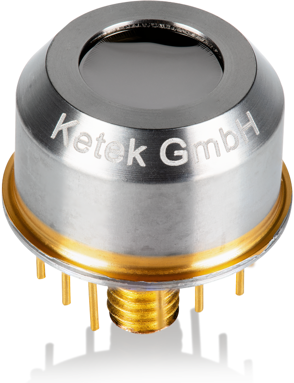
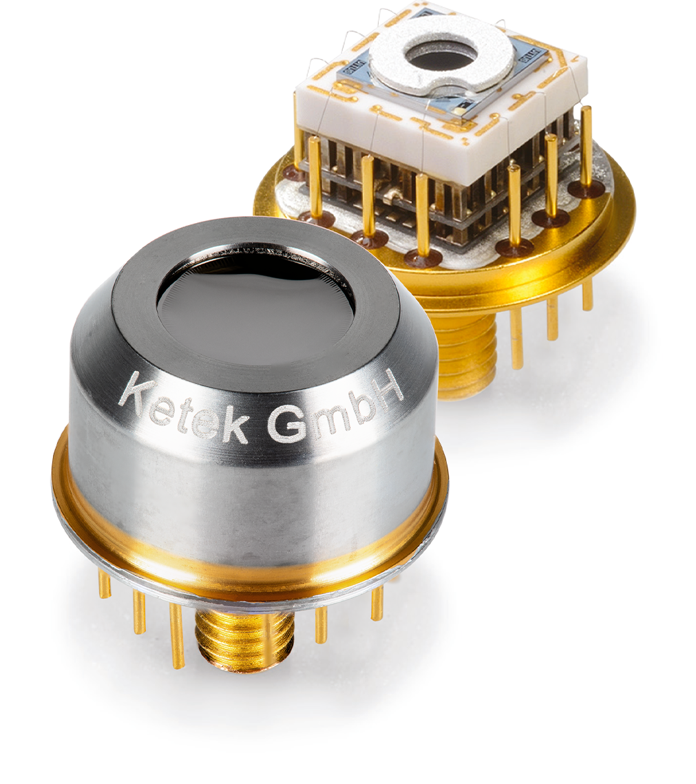
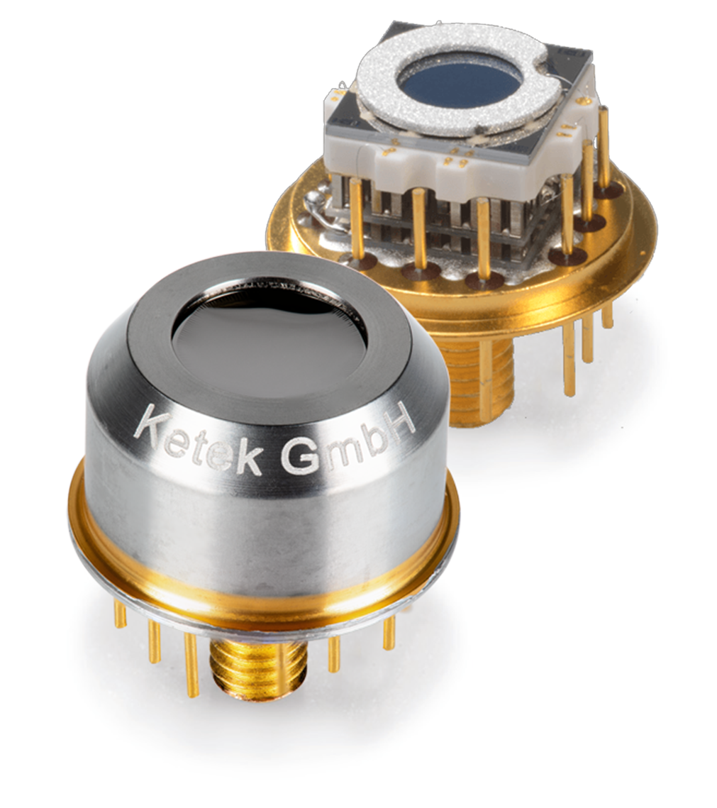
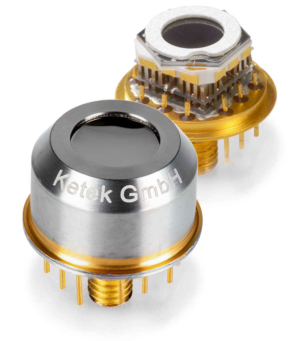
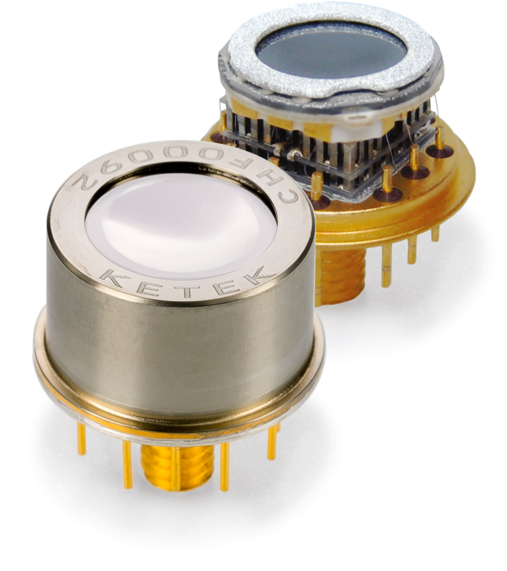
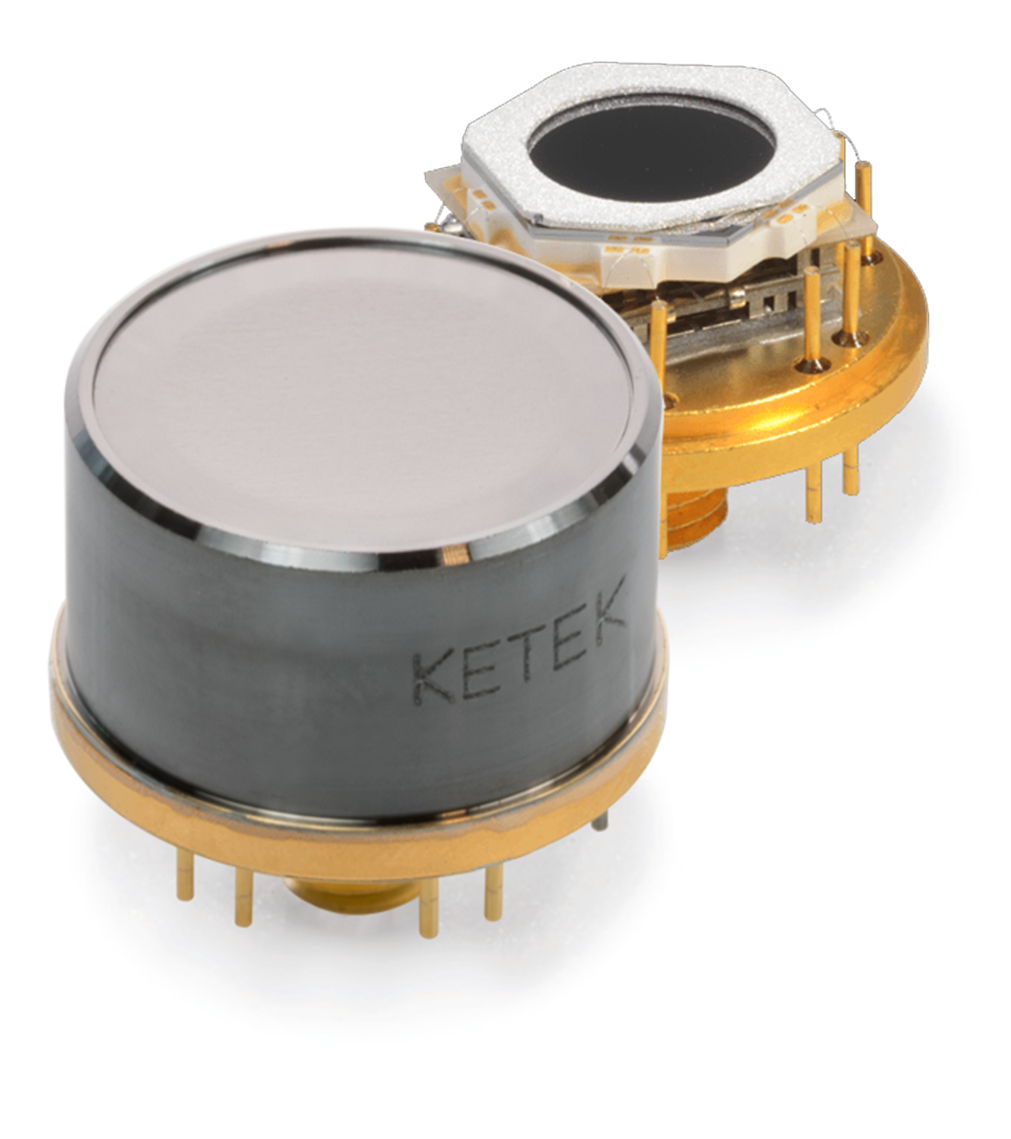
Silicon Drift Detectors
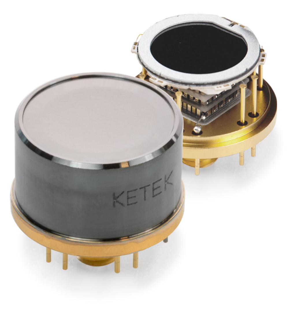
KETEK’s Silicon Drift Detectors (SDD) are the state-of-the-art X-ray sensors for the energy range between 0.05 keV and 30 keV.
They are globally used in manifold applications in electron microscopes, XRF benchtop and XRF handheld spectrometers as well as in material sorting systems for mining and recycling. Due to their wide operating temperature range, their excellent energy resolution, and high reliability they are particularly suited for industrial applications.
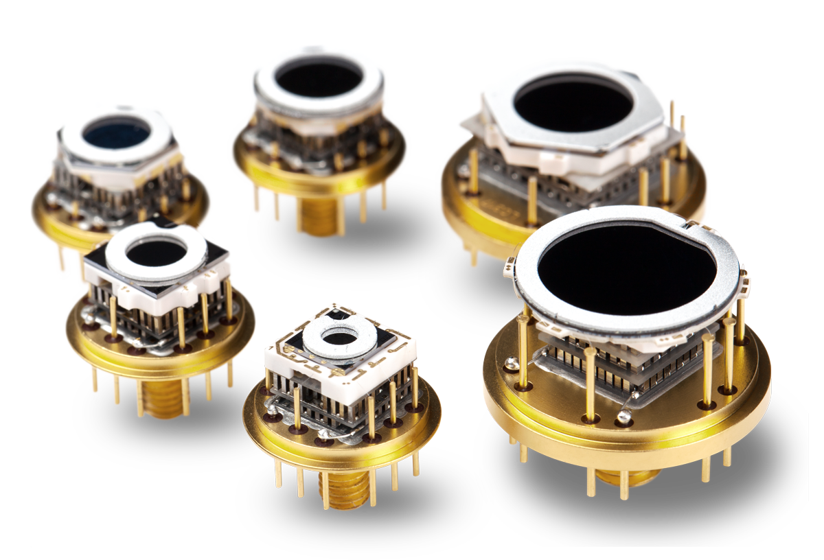
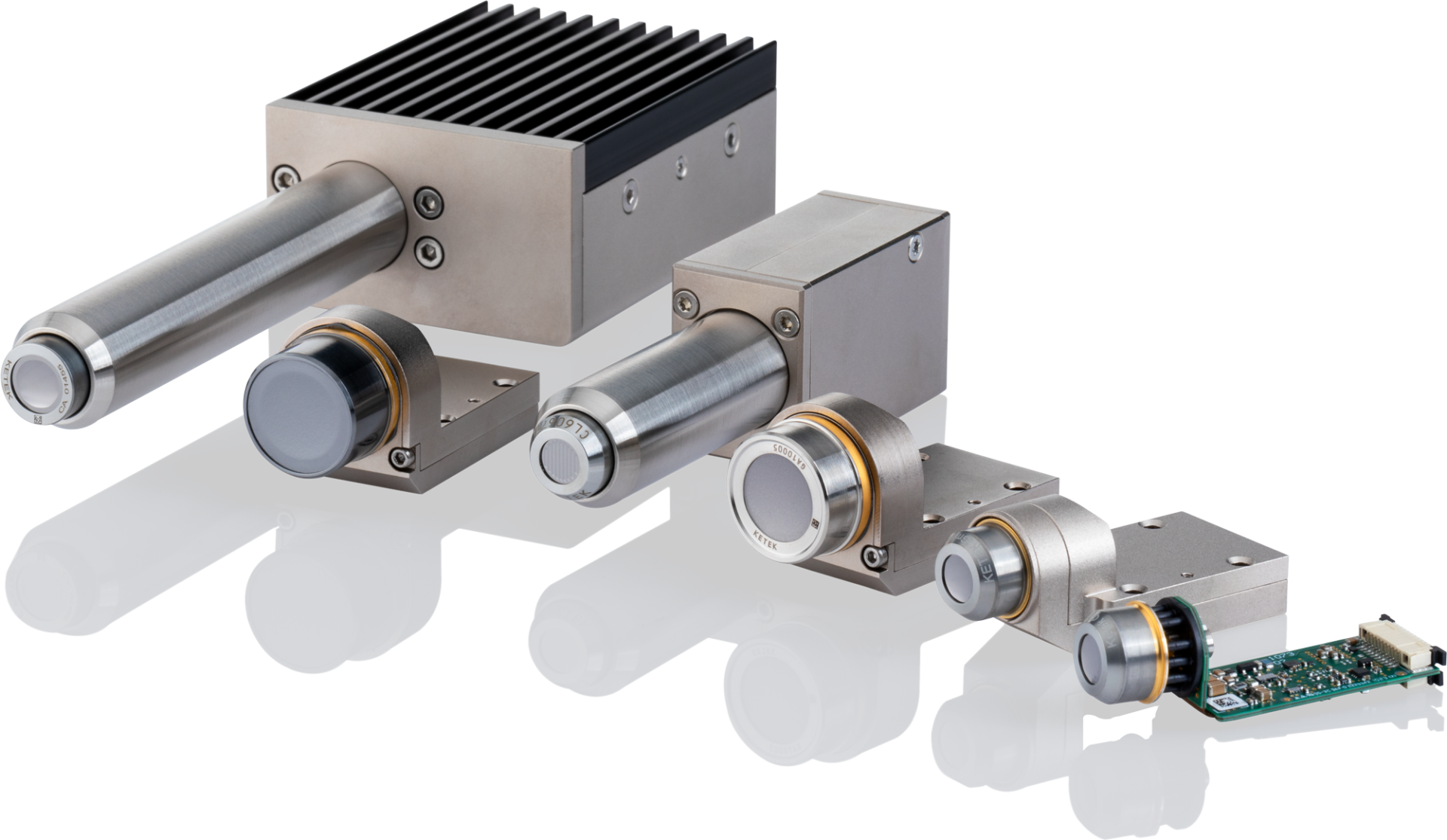
VITUS SDD Series
High-performing Silicon Drift Detectors with collimated areas from 7 mm² to 150 mm² for XRF and EDS applications in industry and science.
Available Options
- CH Window
Standard - CL Window
Low Energy
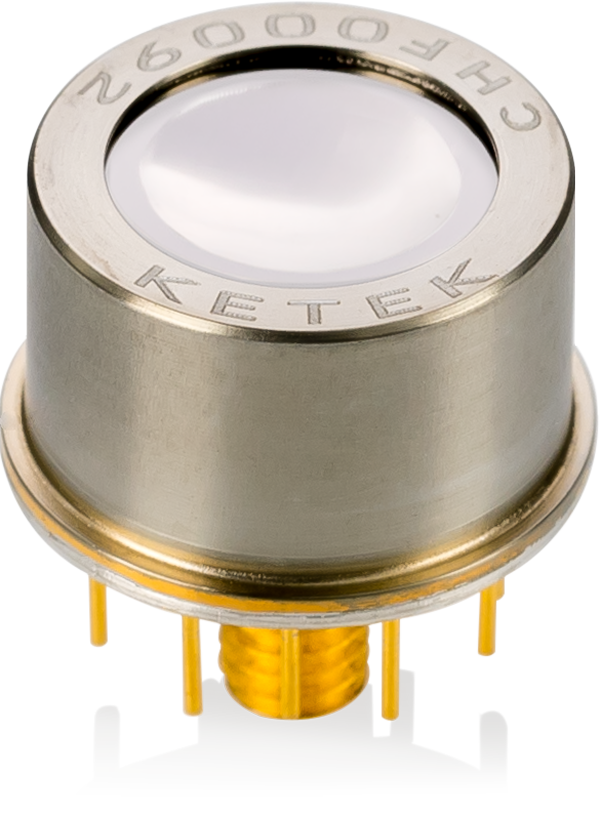
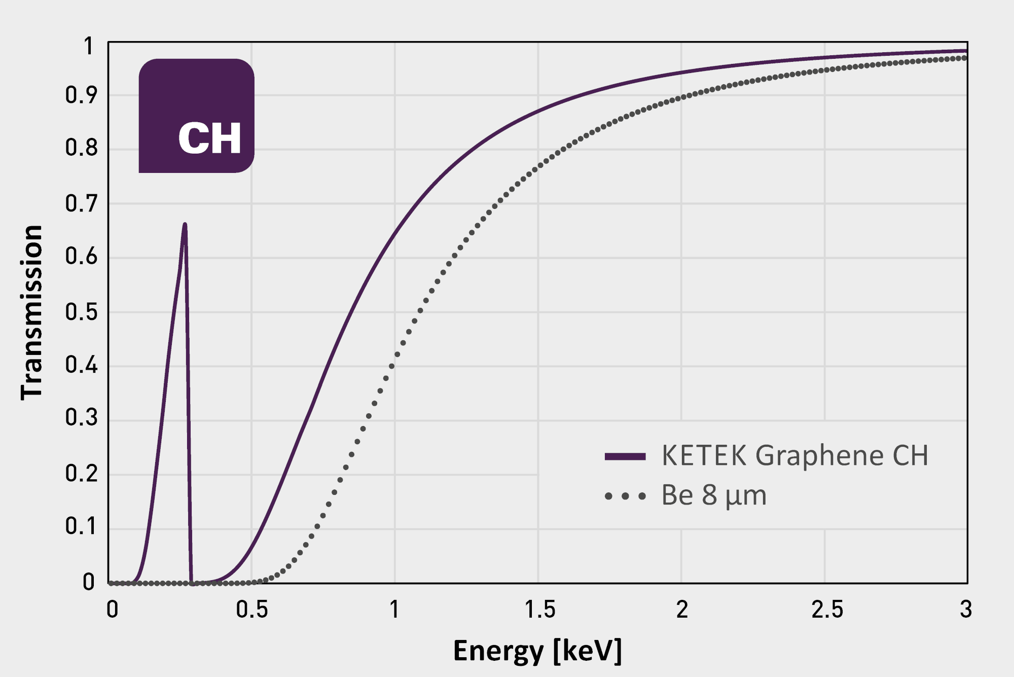
CH Window
1 µm Carbon, replacing 8 µm or 12.5 µm Beryllium
Vacuum encapsulated for many years of stable operation
No window fluorescence lines (pure Carbon)
CL Window
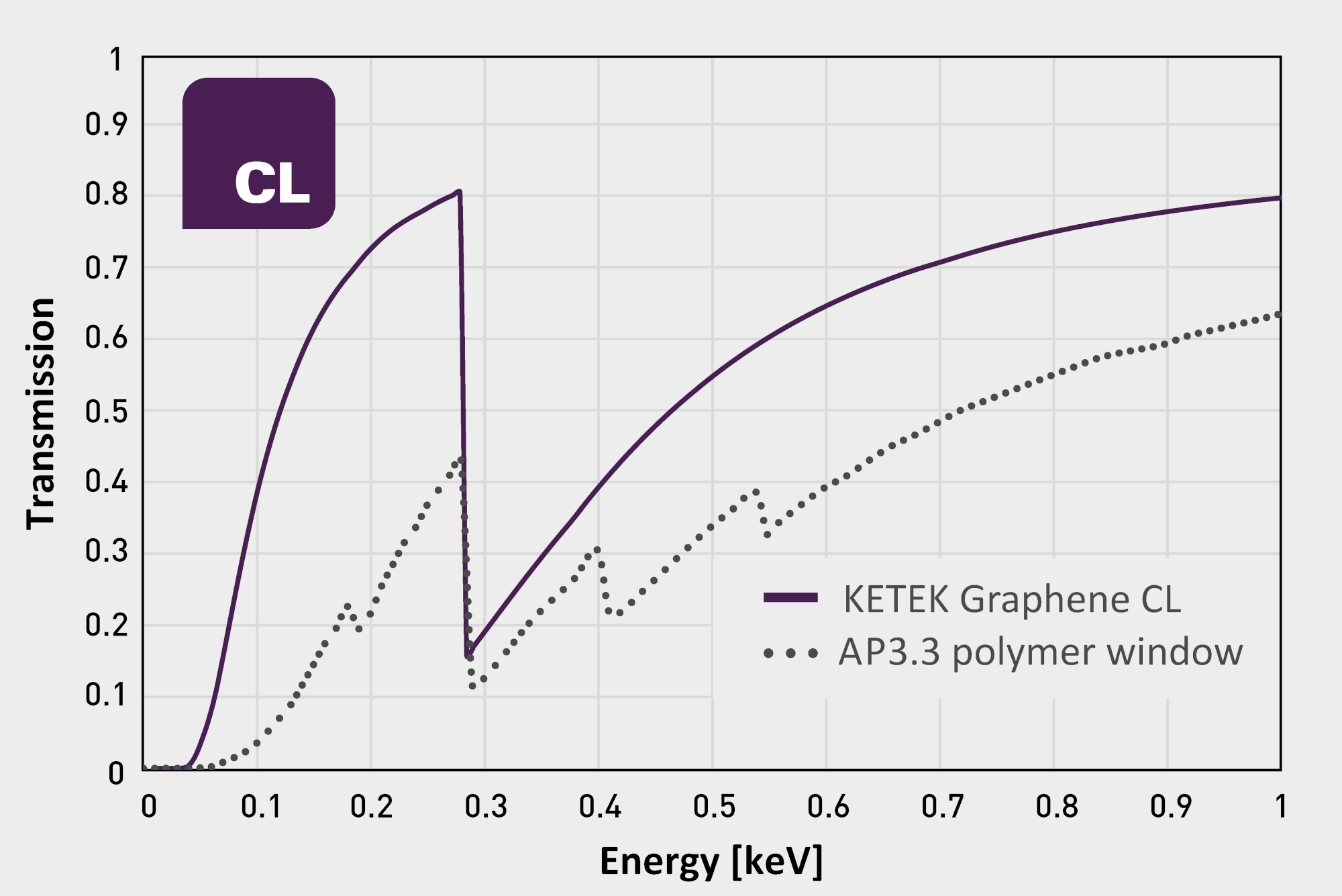
Low-energy type
165 nm Carbon with Silicon support grid
86 % open area
Very high 100° acceptance angle (typical Polymer window: 53°)
Vacuum encapsulated for many years of stable operation
No window fluorescence lines (pure Carbon)
Cooling Performance
- ∆T from 90 K to 130 K depending on heat sink temperature
- Less than 250 mW power consumption at typical operation point (-35 °C chip temperature)
- Power consumption as low as 100 mW possible at 20 °C heat sink and -20 °C chip temperature
- Ultra-stable vacuum integrity for typically more than 10 years of operation
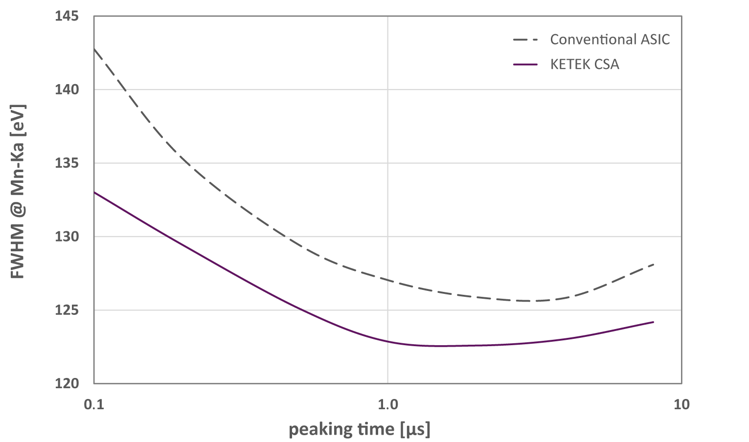
KETEK Proprietary Charge Sensitive Amplifier
- Significantly improved energy resolution, especially at short peaking times
- Extremely high throughput at appropriate DPP settings
Specifications
| Specifications for H7-H150 | |
|---|---|
| First stage amplification | ASIC |
| Energy resolution for H7-H50 and K50 Energy resolution for H80-H150 |
≤ 129 eV @ Mn Kα ≤ 136 eV @ Mn Kα |
| Peak to background | > 15,000 |
| Peak to tail | > 2,000 |
| Optimal peaking time at max. cooling | 1 μs |
| Absorption depth Si for H7 to H150 Absorption depth Si for K50 |
450 µm 550 µm |
| Peak shift stability up to 100 kcps | < 1 eV |
| Max. input count rate | 4,000 kcps |
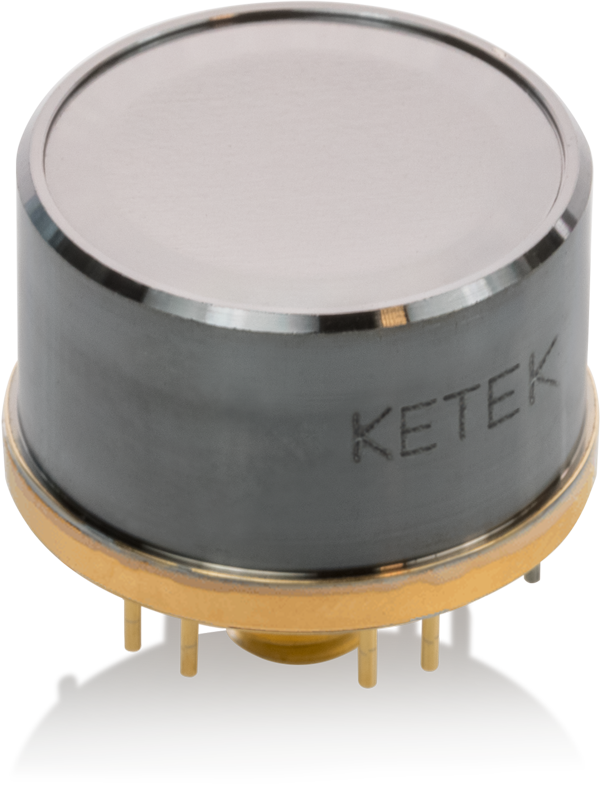
| Window for H7-H50 CH and K50 CH Window for H7-H50 CL and K50 CL Window for H80-H150 |
CH (1 µm Graphene) CL (165 nm Graphene) Be (25 µm Beryllium) |
| Cooling performance | @ +20 °C heat sink ΔT > 95 K |
| On-chip collimator | multilayer |
| Typical SDD parameters | Voltages | Currents |
|---|---|---|
| Ring 1 (R1) | -20 V ± 10 V | 10 µA |
| Ring X (RX) | -130 V ± 30 V | 10 µA |
| Back | -80 V ± 20 V | < 1 nA |
| Peltier element for H7-H50 and K50 |
5.5 V | 600 mA max. |
| Peltier element for H80-H150 |
9 V | 1,000 mA max. |
| Temperature monitor | NTC thermistor 10 kΩ @ 25 °C | |
| Output signal | ramped reset type | |
| Output gain | 1.6 mV/keV ± 20 % | |

